High Definition For Mono-Crystalline 180W Solar Panel for Slovenia Manufacturer
Short Description:
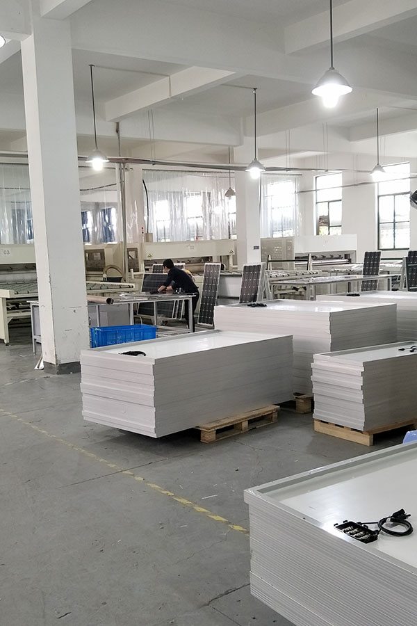
Well-run equipment, professional sales team, and better after-sales services; We are also a unified big family, everyone stick to the company value "unification, dedication, tolerance" for High Definition For Mono-Crystalline 180W Solar Panel for Slovenia Manufacturer, We look forward to establish a long-term business relationship with your esteem co-operation.
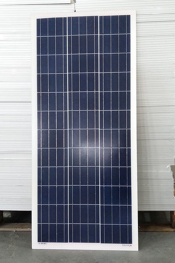
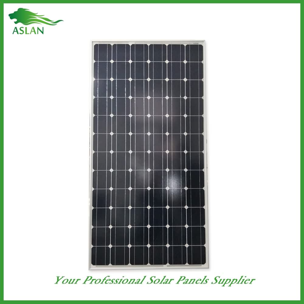
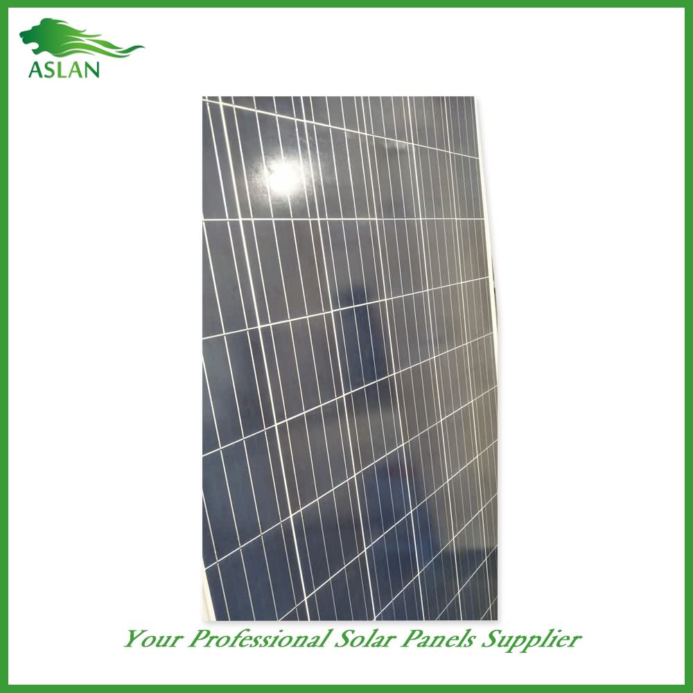
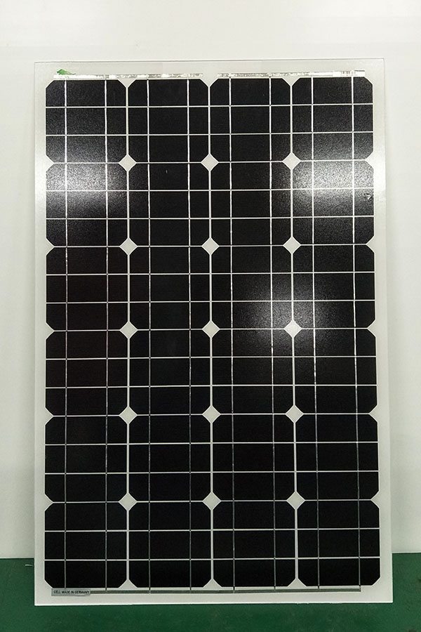
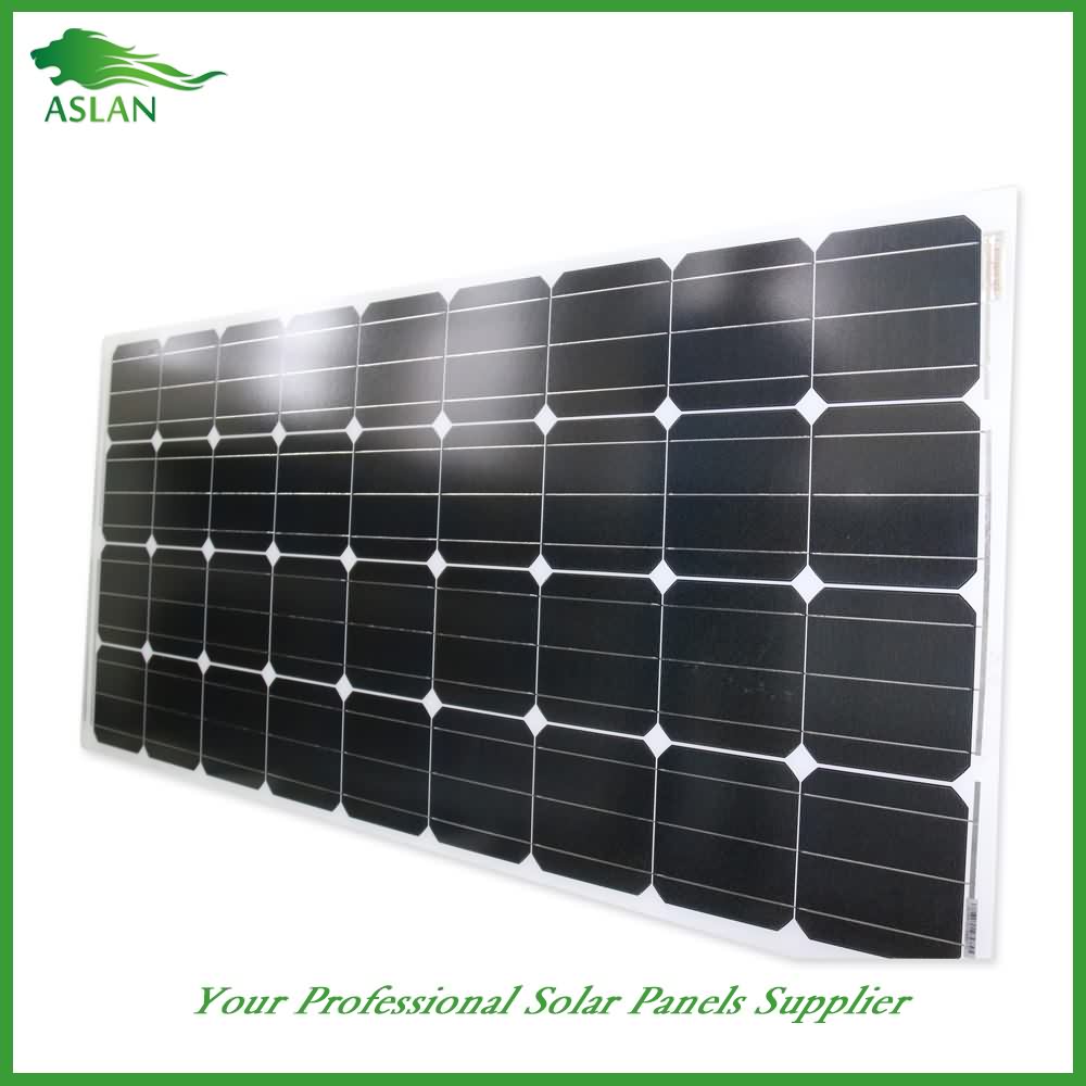
Mono-Crystalline 180W Solar Panel
Technical parameter
Maximum Power(W) 180W
Optimum Power Voltage(Vmp) 36.42V
Optimum Operating Current(Imp) 4.96A
Open Circuit Voltage(Voc) 44.45V
Short Circuit Current(Isc) 5.44A
Mechanical Characteristics
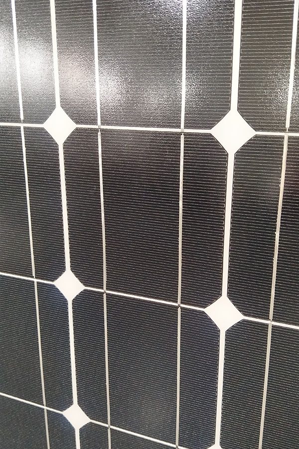
Cell Type Mono-crystalline 125x125mm (5 inch)
No of Cell 72 (6x12pcs)
Dimensions 1580x808x35mm
Weight 14.5Kg
Front Glass 3.2mm,High Transmission, Low Iron,Tempered Glass
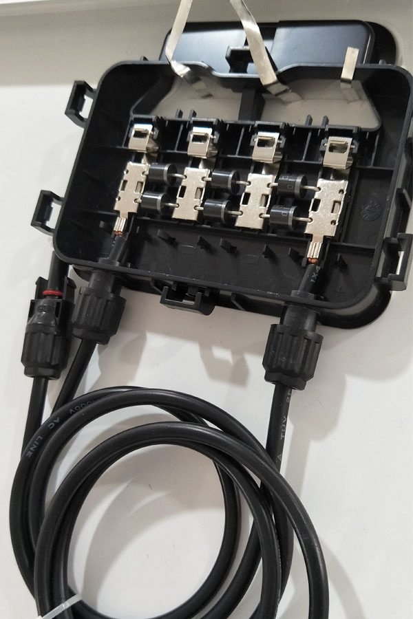
Junction box IP65 Rated
Output Cable TUV 1×4.0mm2/UL12AWG,Length:900mm
Temperature and Coefficients
Operating Temperature(°C): -40°C ~ + 85°C
Maximum System Voltage: 600V(UL)/1000V(IEC) DC
Maximum Rated Current Series: 15A
Temperature Coefficients of Pmax: -0.47%
Temperature Coefficients of Voc: -0.389%
Temperature Coefficients of Isc: 0.057%
Nominal Operationg Cell Temperature (NOCT): 47+/-2°C
Materials of solar panel
1).Solar Cell——Mono-crystalline solar cell 125*125mm
2).Front Glass——-3.2mm, high transmission, low iron, tempered glass
3).EVA——-excellent anti-aging EVA
4).TPT——-TPT hot seal made of flame resistance
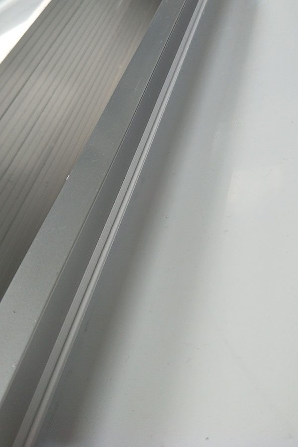
5).Frame——anodized aluminum profile
6).Junction Box——-IP65 rated, high quality, with diode protection
Superiority: high quality anodized aluminum frame, high efficiency long life, easy installation, strong wind resistance, strong hail resistance.
Features
1. High cell efficiency with quality silicon materials for long term output stability
2. Strictly quality control ensure the stability and reliability, totally 23 QC procedures
3. High transmittance low iron tempered glass with enhanced stiffness and impact resistance
4. Both Poly-crystalline and Mono-crystalline
5. Excellent performance in harsh weather
6. Outstanding electrical performance under high temperature and low irradiance
Quality assurance testing
Thermal cycling test
Thermal shock test
Thermal/Freezing and high humidity cycling test
Electrical isolation test
Hail impact test
Mechanical, wind and twist loading test
Salt mist test
Light and water-exposure test
Moist carbon dioxide/sulphur dioxide
In This video we see that how can use that of solar panel about the more facilities like SunRaiden Easy-to-use 300W solar Inverter charger and 3W Led and ORANGELINK wifi contollable auto dog feeder with camera , Wifi IP camera .
And Please Subscribe Our Channel and click on red buttonn
What is AMORPHOUS SILICON? What does AMORPHOUS SILICON mean? AMORPHOUS SILICON meaning – AMORPHOUS SILICON definition – AMORPHOUS SILICON explanation.
Source: Wikipedia.org article, adapted under https://creativecommons.org/licenses/by-sa/3.0/ license.
Amorphous silicon (a-Si) is the non-crystalline form of silicon used for solar cells and thin-film transistors in LCD displays.
Used as semiconductor material for a-Si solar cells, or thin-film silicon solar cells, it is deposited in thin films onto a variety of flexible substrates, such as glass, metal and plastic. Amorphous silicon cells generally feature low efficiency, but are one of the most environmentally friendly photovoltaic technologies, since they do not use any toxic heavy metals such as cadmium or lead.
As a second-generation thin-film solar cell technology, amorphous silicon was once expected to become a major contributor in the fast-growing worldwide photovoltaic market, but has since lost its significance due to strong competition from conventional crystalline silicon cells and other thin-film technologies such as CdTe and CIGS.
Amorphous silicon differs from other allotropic variations, such as monocrystalline silicon—a single crystal, and polycrystalline silicon, that consists of small grains, also known as crystallites.
Silicon is a fourfold coordinated atom that is normally tetrahedrally bonded to four neighboring silicon atoms. In crystalline silicon (c-Si) this tetrahedral structure continues over a large range, thus forming a well-ordered crystal lattice.
In amorphous silicon this long range order is not present. Rather, the atoms form a continuous random network. Moreover, not all the atoms within amorphous silicon are fourfold coordinated. Due to the disordered nature of the material some atoms have a dangling bond. Physically, these dangling bonds represent defects in the continuous random network and may cause anomalous electrical behavior.
The material can be passivated by hydrogen, which bonds to the dangling bonds and can reduce the dangling bond density by several orders of magnitude. Hydrogenated amorphous silicon (a-Si:H) has a sufficiently low amount of defects to be used within devices such as solar photovoltaic cells, particularly in the protocrystalline growth regime. However, hydrogenation is associated with light-induced degradation of the material, termed the Staebler–Wronski effect.
Amorphous alloys of silicon and carbon (amorphous silicon carbide, also hydrogenated, a-Si1-xCx:H) are an interesting variant. Introduction of carbon atoms adds extra degrees of freedom for control of the properties of the material. The film could also be made transparent to visible light.
Increasing concentrations of carbon in the alloy widen the electronic gap between conduction and valence bands (also called “optical gap” and bandgap). This can potentially increase the light efficiency of solar cells made with amorphous silicon carbide layers. On the other hand, the electronic properties as a semiconductor (mainly electron mobility), are adversely affected by the increasing content of carbon in the alloy, due to the increased disorder in the atomic network.
Several studies are found in the scientific literature, mainly investigating the effects of deposition parameters on electronic quality, but practical applications of amorphous silicon carbide in commercial devices are still lacking.
Unhydrogenated a-Si has a very high defect density which leads to undesirable semiconductor properties such as poor photoconductivity and prevents doping which is critical to engineering semiconductor properties. By introducing hydrogen during the fabrication of amorphous silicon, photoconductivity is significantly improved and doping is made possible. Hydrogenated amorphous silicon, a-Si:H, was first fabricated in 1969 by Chittick, Alexander and Sterling by deposition using a silane gas (SiH4) precursor. The resulting material showed a lower defect density and increased conductivity due to impurities. Interest in a-Si:H came when (in 1975), LeComber and Spear discovered the ability for substitutional doping of a-Si:H using phosphine (n-type) or diborane (p-type). The role of hydrogen in reducing defects was verified by Paul’s group at Harvard who found a hydrogen concentration of about 10 atomic % through IR vibration, which for Si-H bonds has a frequency of about 2000 cm-1. Starting in the 1970′s, a-Si:H was developed in solar cells by RCA by which steadily climbed in efficiency to about 13.6% in 2015.