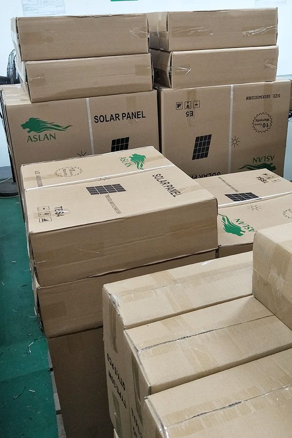
Factory directly sale Poly-crystalline Solar Panel 40W Uzbekistan Factory
Short Description:
Assume full responsibility to meet all demands of our clients; achieve continuous advancements by promoting the growth of our clients; become the final permanent cooperative partner of clients and maximize the interests of clients for Factory directly sale Poly-crystalline Solar Panel 40W Uzbekistan Factory, Our professional technical team will be wholeheartedly at your service. We sincerely welcome you to visit our website and company and send us your inquiry.
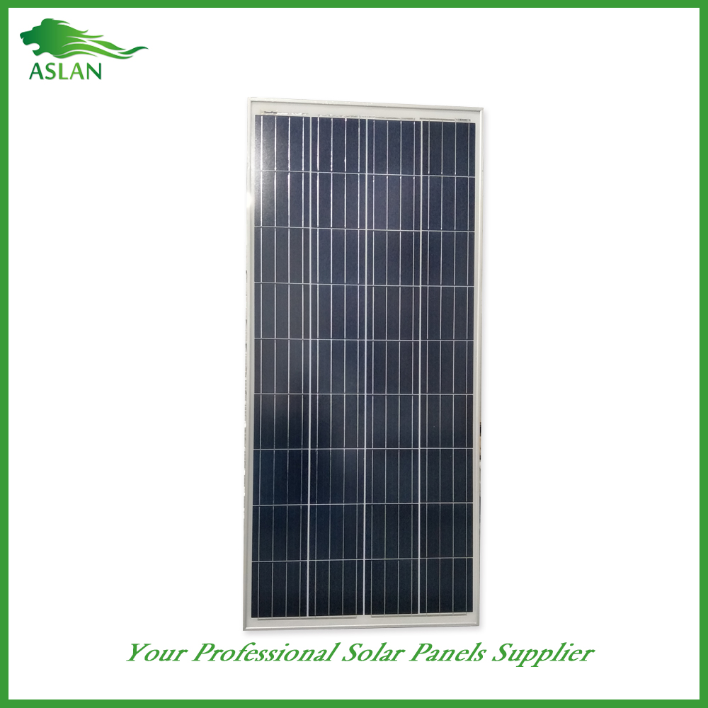
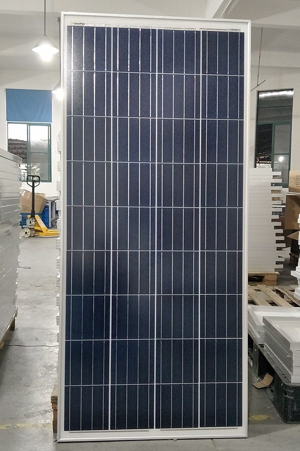
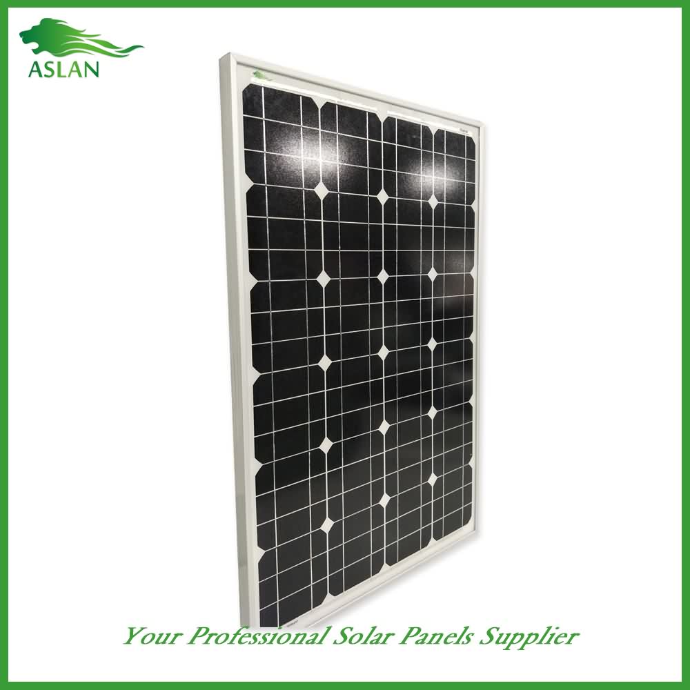
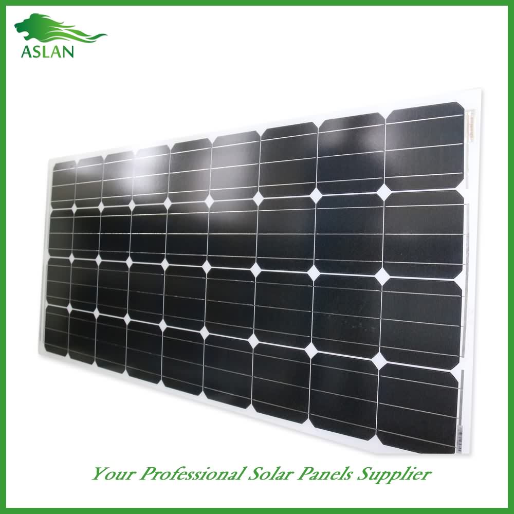
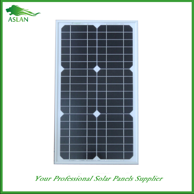
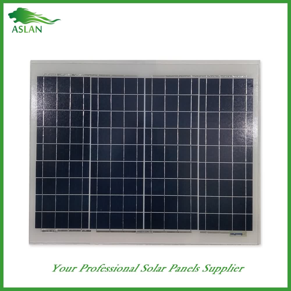
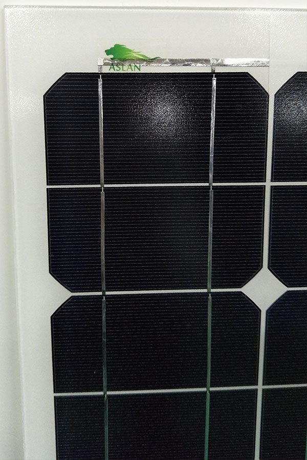
Poly-crystalline Solar Panel 40W
Technical parameter
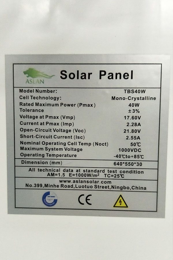
Maximum Power(W) 40W
Optimum Power Voltage(Vmp) 17.35V
Optimum Operating Current(Imp) 2.31A
Open Circuit Voltage(Voc) 21.16V
Short Circuit Current(Isc) 2.53A
Mechanical Characteristics
Cell Type Polycrystalline 156 x 52mm
No of Cell 36 (4x9pcs)
Dimensions 670x420x30mm
Weight 4.0Kg
Front Glass 3.5mm,High Transmission, Low Iron,Tempered Glass
Junction box IP65 Rated
Output Cable TUV 1×4.0mm2/UL12AWG,Length:900mm
Temperature and Coefficients
Operating Temperature(°C): -40°C ~ + 85°C
Maximum System Voltage: 600V(UL)/1000V(IEC) DC
Maximum Rated Current Series: 15A
Temperature Coefficients of Pmax: -0.47%
Temperature Coefficients of Voc: -0.389%
Temperature Coefficients of Isc: 0.057%
Nominal Operationg Cell Temperature (NOCT): 47+/-2°C
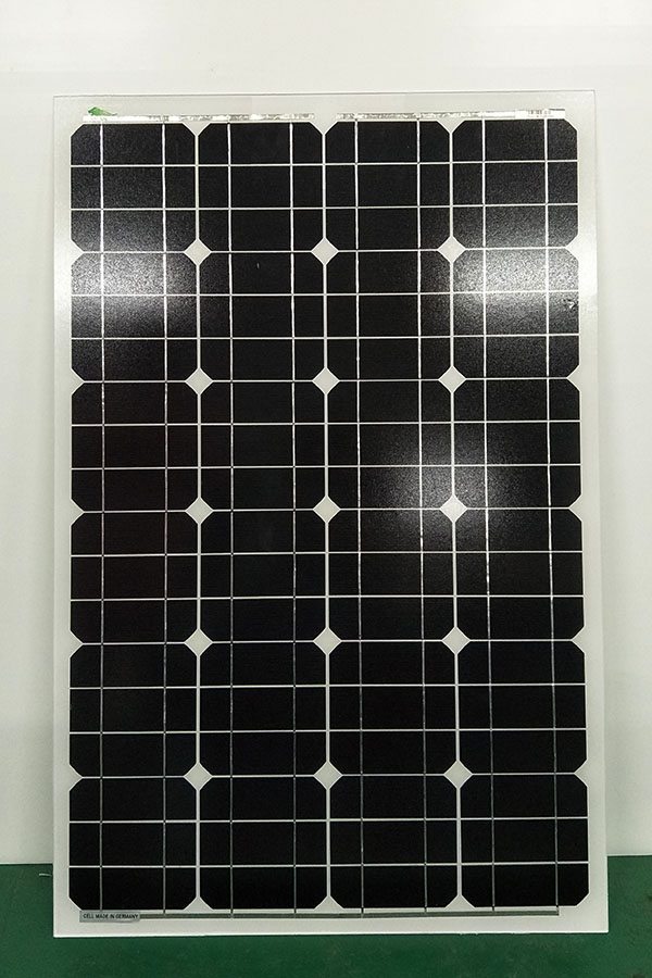
Materials of solar panel
1).Solar Cell——Polycrystalline solar cell 156*52mm
2).Front Glass——-3.2mm, high transmission, low iron, tempered glass
3).EVA——-excellent anti-aging EVA
4).TPT——-TPT hot seal made of flame resistance
5).Frame——anodized aluminum profile
6).Junction Box——-IP65 rated, high quality, with diode protection
Superiority: high quality anodized aluminum frame, high efficiency long life, easy installation, strong wind resistance, strong hail resistance.
Features
1. High cell efficiency with quality silicon materials for long term output stability
2. Strictly quality control ensure the stability and reliability, totally 23 QC procedures
3. High transmittance low iron tempered glass with enhanced stiffness and impact resistance
4. Both Poly-crystalline and Mono-crystalline
5. Excellent performance in harsh weather
6. Outstanding electrical performance under high temperature and low irradiance
Quality assurance testing
Thermal cycling test
Thermal shock test
Thermal/Freezing and high humidity cycling test
Electrical isolation test
Hail impact test
Mechanical, wind and twist loading test
Salt mist test
Light and water-exposure test
Moist carbon dioxide/sulphur dioxide
สนใจติดต่อ ร้าน Power.intown
Inbox กด http://m.me/power.intown
Line กด http://line.me/ti/p/6Med9Hbhtw
Tel กด 09-5253-0057 (12.00-24.00 เที่ยงวัน-เที่ยงคืน)
.
ข้อมูลสินค้า กด http://powerintown.lnwshop.com/
รีวืว กด https://www.youtube.com/channel/UCLF2XnBQvFBgj1U7cznO6QQ
https://www.fiberoptics4sale.com
Most of today’s electronic devices are made with single crystal silicon. But silicon never occurs alone in nature as an element, so how do we make it?
Silicon is the second most abundant element in the earth’s crust, but they mainly exist as silica, impure SiO2, and silicates, Si + O + another element. Normal sand and the sand used in the building industry is usually colored red, yellow or orange due to the presence of impurities, and we don’t use them. Instead, what we need is silica sand, or high purity quartz rock, which we get from quarrying. Ideally the silica has low concentrations of iron, aluminum and other metals.
The process of silicon purification is illustrated in this flow chart.
The silica sand powder is heated together with carbon in an electric furnace to 1,800°C. Carbon pulls the oxygen away from silicon dioxide and becomes carbon dioxide, leaving behind low-grade impure silicon. The silicon is then treated with oxygen to remove impurities such as calcium or aluminum, leaving up to 99% pure silicon.
This silicon is still not pure enough for semiconductor chipmakers. So it is ground into a fine powder, mixed with hydrogen chloride and heated at 300 degrees C. This process yields Trichlorosilane , HSiCl3, a liquid at room temperature.
The above process also creates chlorides of unwanted elements such as iron, aluminum, boron and phosphorus. The HSiCl3 has a low boiling point of 31.8 °C and distillation is used to purify the HSiCl3 from theimpurity halides.
Then this high-purity trichlorosilane, HSiCl3, is vaporized in hydrogen atmosphere at 1,100 degrees C for 200~300 hours. The reaction takes place inside large vacuum chambers and the silicon is deposited onto electrically heated thin polysilicon rods, small grain size silicon, to produce high-purity polysilicon rods of diameter 150-200mm. This electronic-grade silicon has purity of 99.999999%, eight nines.
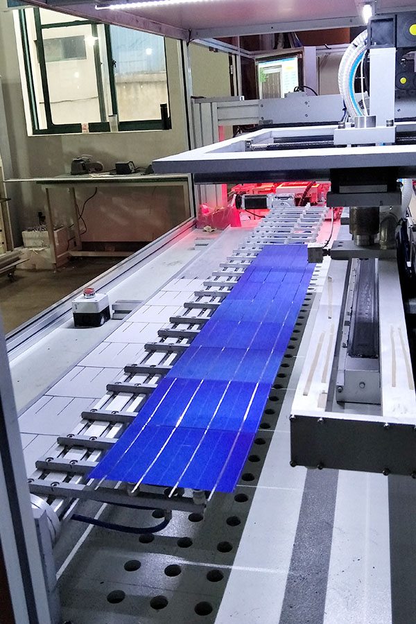
The previous steps produced ultra-pure silicon, however, it is not single crystal silicon, crystalline, instead it is polysilicon, polycrystalline, and is composed of lots of small silicon crystals and the boundaries between them can cause trouble with electronic signals. So we have to convert it to large single crystal silicon, crystalline.
The resulting polysilicon rods from last page are broken up to feed the crystallization process. This process is called the Czochralski method.
The ultra-pure polycrystalline silicon is placed in a quartz crucible and molten in an inert atmosphere.
A small single crystal, or Si “seed” crystal, is clamped to a metal rod with the normal to its bottom carefully aligned along a pre-determined direction, typically 111 or 100 direction.
The “seed” crystal is dipped into the melt. Once thermal equilibrium is achieved, the temperature of the melt close to the seed crystal is reduced, and silicon from the melt begins to freeze out onto the seed crystal, forming a perfect extension of the seed crystal.
The seed crystal is slowly rotated in the opposite direction to the rotation of the crucible and withdrawn from the melt; this allows more and more silicon to freeze out on the bottom of the growing crystal.
The resulting large, cylindrically shaped single crystal of silicon is typically 4 to 6 inches in diameter and 1 to 2 meters in length.
We will briefly introduce the process for making silicon wafers used for semiconductor device fabrication.
First, the cylindrical single crystal silicon rod is cut with diamond-edged saw to create very thin wafers. The sharp edges are then smoothed to prevent from chipping.
The wafers surfaces are polished using an abrasive slurry until the wafers are flat to a tolerance of two thousandths of a millimeter.
The wafer is then etched with a mixture of nitric, hydrofluoric and acetic acids to create an even smoother surface.